DMI – Graduate Course in Computer Science
Copyleft
![]() 2018 Giuseppe Scollo
2018 Giuseppe Scollo
![]()
precursors: PLA, PAL, CPLD
typical FPGA constituents:
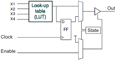
a model of a programmable logic block
configuration of the block in the figure:
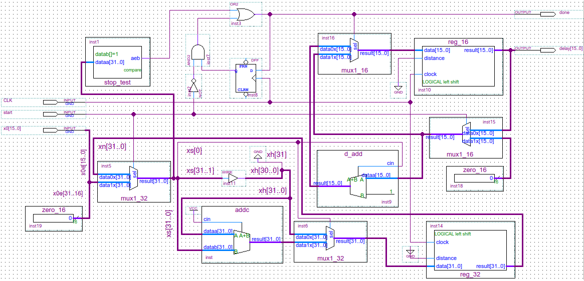
schematic using library parameterized modules (lpm)
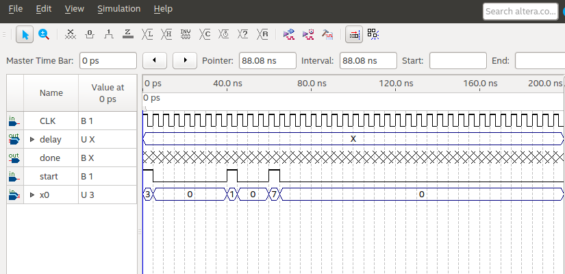
simulation testbench for the Collatz delay datapath
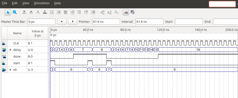
simulation outcome for the Collatz delay datapath