DMI – Graduate Course in Computer Science
Copyleft
![]() 2019 Giuseppe Scollo
2019 Giuseppe Scollo
![]()
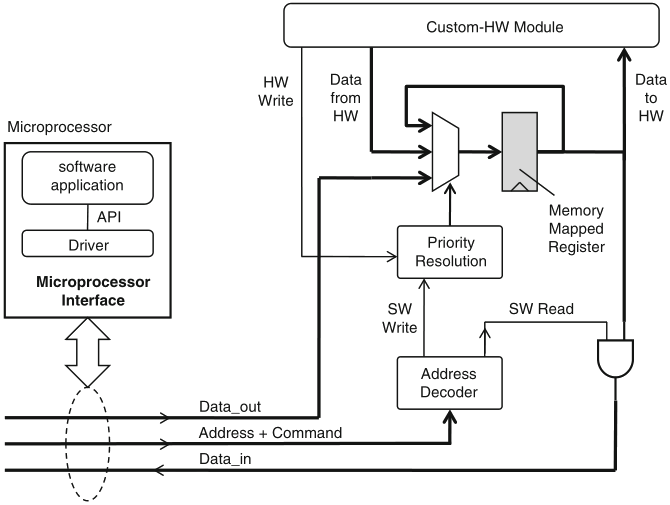
memory-mapped interfaces are the most general type of HW/SW interface
Schaumont, Figure 11.1 - A memory-mapped register
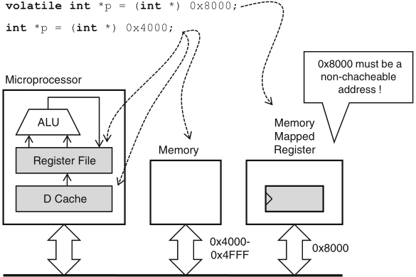
why must the pointer be a volatile pointer?
Schaumont, Figure 11.2 - Integrating a memory-mapped register in a memory hierarchy
however, defining a memory-mapped register with a volatile pointer will not prevent that memory address from being cached!
two approaches to deal with this problem:
simple extension of a memory-mapped register with a handshake mechanism, whereby the communicating parties signal the register state to each other
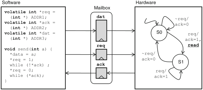
Schaumont, Figure 11.3 - A mailbox register between hardware and software
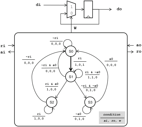
the protocol shown in the figure has two synchronization points, viz. just after req and ack taking the same value
two main disadvantages of this protocol:
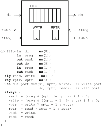
the use of a FIFO queue compensates temporary imbalances between the read and write throughputs
instead of controlling access to a single register, a single handshake can also be used to control access to a region of memory
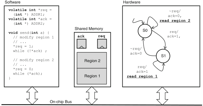
Schaumont, Figure 11.6 - A double-buffered shared memory with a memory-mapped request/acknowledge handshake
in one phase of the protocol in figure, changes are allowed to region 1 of the memory, while in the other phase of the protocol, changes are allowed in region 2 of the memory
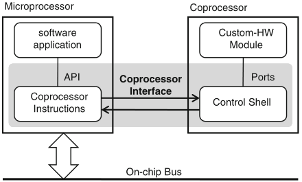
Schaumont, Figure 11.7 - Coprocessor interface
when high data-throughput between the software and the custom hardware is needed, a dedicated processor interface outperforms memory-mapped interfaces
both the coprocessor instruction set and the specific coprocessor interface depend on the type of processor—not all processors have a coprocessor interface
main advantages of a coprocessor interface over an on-chip bus:
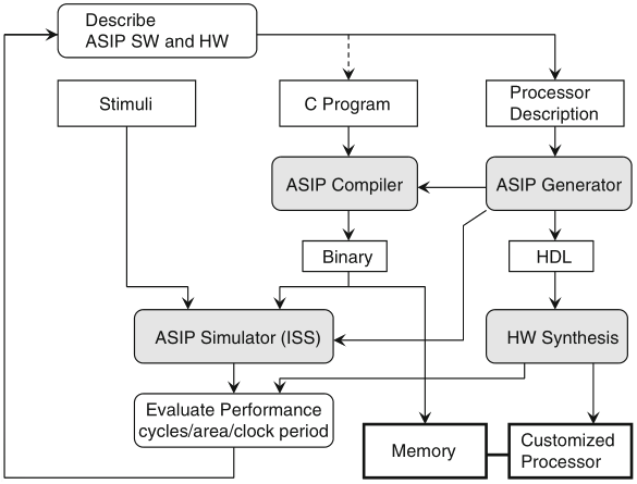
Schaumont, Figure 11.12 - ASIP design flow
sequential ASIP design does not generally deliver better performance than SoC design based on custom hardware modules, yet it does deliver less error-prone results
the Nios-II softcore processor has a coprocessor interface whereby custom instructions may be defined and hardware modules may be attached to
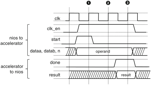
Schaumont, Figure 11.15 - Nios-II custom-instruction interface timing
the interface supports variable-length execution of custom instructions through a two-way handshake
the clk_en input is used to mask off the clock to the custom hardware when the instruction is inactive
the use of a local register file in the custom hardware module is also supported
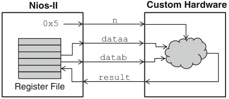
Schaumont, Figure 11.16a - Nios-II custom-instruction integration with processor register file
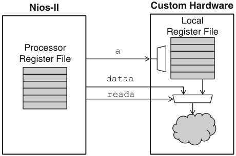
Schaumont, Figure 11.16b - Nios-II custom-instruction integration with local register file
a custom instruction may take operands from either register file: registers prefixed with r are located in the processor, while registers prefixed with c are located in the custom hardware
figure 11.16b shows the case for the first input operand only: the control signal reada selects either the processor's or the local register file